应用方向知识库 03Application Knowledge 03

按专业方向进入,再匹配合适的工艺资源。Enter by application field, then match the right process resources.

做光学、MEMS、微流控、传感电极、新材料和量子器件时,真正有用的不是一句“能做”,而是先把应用目标、材料限制、关键尺寸和验收方式拆清楚。For optics, MEMS, microfluidics, sensors, electrodes, emerging materials and quantum devices, the useful answer is not a quick yes. It is a clear split of goal, material limits, critical dimensions and acceptance method.

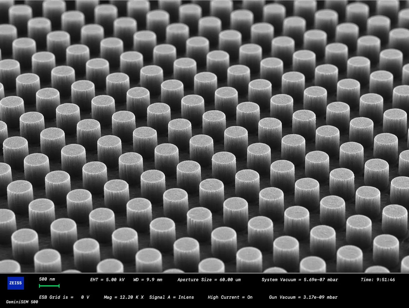
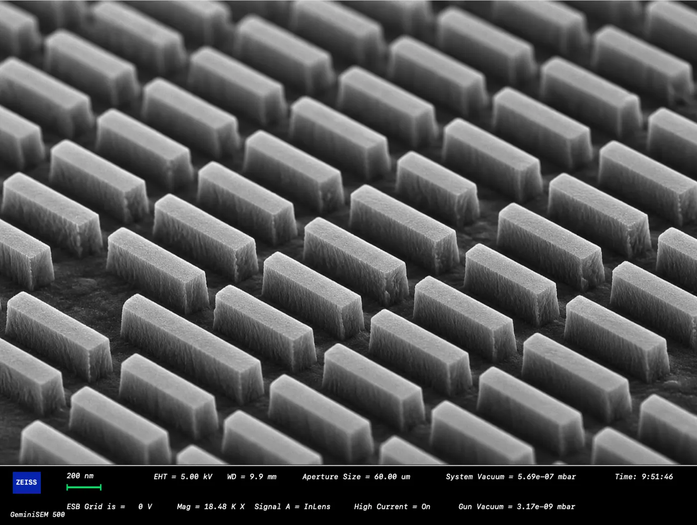
SEM image of nano pillar array
Photonics / Optics

光学与光子器件Photonics and Optical Devices

超表面、超透镜、波导、光栅、衍射光学元件,重点确认波长、材料折射率、结构高度、周期和测试方式。Metasurfaces, metalenses, waveguides, gratings and diffractive optics. Confirm wavelength, index, height, period and metrology.

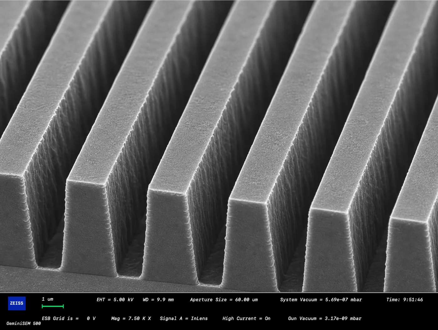
SEM image of deep silicon trenches
MEMS / Microfluidics

MEMS 与微流控MEMS and Microfluidics

微通道、腔体、深硅刻蚀、玻璃/PDMS、键合封装,提前考虑深宽比、泄漏和连接方式。Microchannels, cavities, deep silicon etch, glass/PDMS and bonding. Check aspect ratio, leakage and connection.

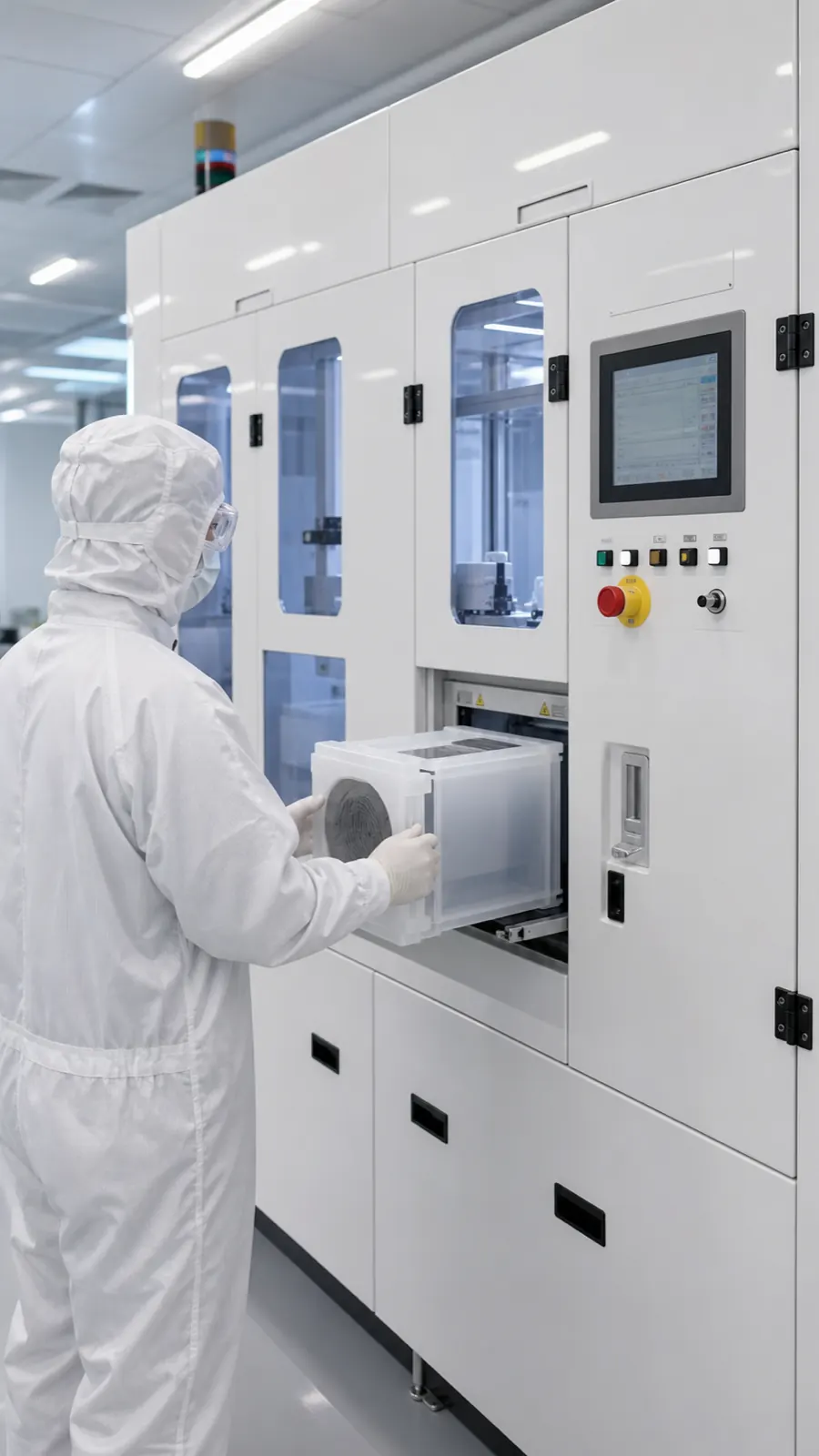
Semiconductor wafer process equipment
Sensor / Electrode

传感器与电极Sensors and Electrodes

叉指电极、微电极、功能薄膜、钝化开窗和电学测试,重点看附着、残胶、接触电阻和测试可达性。IDEs, microelectrodes, functional films, passivation windows and electrical tests. Watch adhesion, residue, resistance and access.

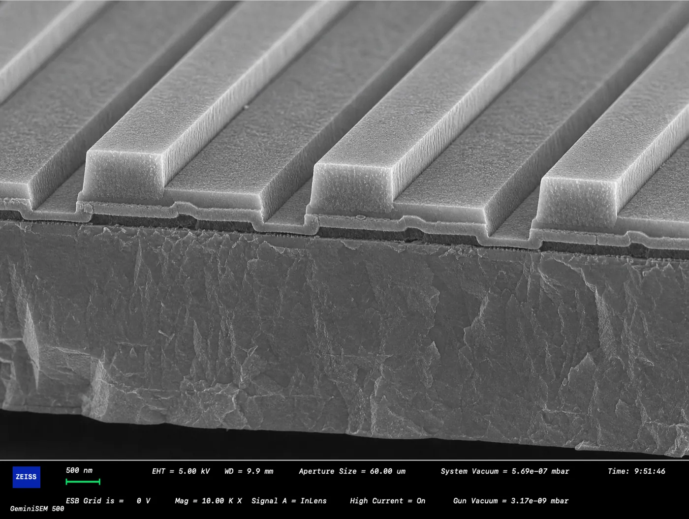
SEM cross-section of device structure
Materials / Quantum

新材料与量子器件Emerging Materials and Quantum Devices

二维材料、SiN、AlN、III-V 和低损伤器件,先列出温度、等离子、溶剂、充电和污染限制。2D materials, SiN, AlN, III-V and low-damage devices. Start with temperature, plasma, solvent, charging and contamination limits.

SEM image of nanoscale grating array
Grating / Imprint

光栅、母版与周期阵列Gratings, Masters and Periodic Arrays

周期阵列和母版类需求可进入纳米压印与母版页面,重点看周期、占空比、面积、缺陷和复制方式。For periodic arrays and masters, review period, duty cycle, area, defects and replication method.

先说明应用目标Describe the Application Goal

例如用于成像、耦合、传感、过滤、流体控制、电学测试、封装连接还是结构验证。目标越明确,越容易判断哪些参数必须保住,哪些参数可以让工艺侧优化。Explain whether it is for imaging, coupling, sensing, filtering, fluid control, electrical tests, packaging connection or structural validation. Clear goals reveal which parameters are fixed and which can be optimized.

再匹配工艺组合Then Match Process Mix

根据应用目标,选择光刻、刻蚀、镀膜、Lift-off、键合、减薄、压印或测试组合,而不是只看单个工艺名称。需求说得越具体,越容易匹配合适的平台、公司或供应商。Match lithography, etch, films, lift-off, bonding, thinning, imprint or testing as a process mix, not one isolated process name. Better input makes better supplier matching.